Availability: | |
---|---|
Quantity: | |
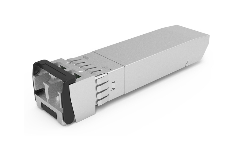
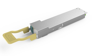
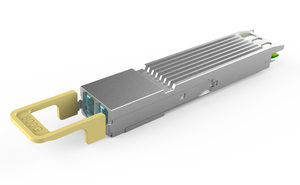
25G SFP28 SR Transceiver
zhaolong
Application
Data center & Networking Equipment
Servers/Storage Devices
High Performance Computing (HPC)
Switches/Routers
Telecom Central Offices (CO)
Test and Measurement Equipment
Standards Compliance
IEEE 802.3ae
SFF8472
SFP+ MSA
SFF-8431 and SFF-8432
Features
Up to 11.1Gbps Data Links
850nm VCSEL laser and PIN receiver
Operating case temperature: (0℃~70℃)
Maximum link length of 300m via OM3 multimode Fiber (MMF)
Operating temperature range:
Commercial: 0℃ to +70℃
Industrial: -40℃ to +85℃
Product Specification
Absolute Maximum Ratings (TC=25℃, unless otherwise noted)
Stresses in excess of the absolute maximum ratings can cause permanent damage to the device. These are absolute stress ratings only. Functional operation of the device is not implied at these or any other conditions in excess of those given in the operational sections of the data sheet. Exposure to absolute maximum ratings will cause permanent damage and/or adversely affect device reliability.
Parameter | Symbol | Min | Typical | Max | Unit | Notes |
Storage Temperature | TS | -40 | - | +85 | ºC | |
Operating Relative Humidity | RH | 0 | - | +85 | % | No condensation |
Parameter | Symbol | Min | Typical | Max | Unit | Notes |
Operating Case Temperature | Tc | 0 | - | 70 | ºC | |
Power Supply Voltage | Vcc | 3.15 | 3.3 | 3.45 | V | |
Lane Baud Rate | BRLANE | 10.3125 | Gbps |
Electrical Characteristics
Parameter | Symbol | Min | Typical | Max | Unit | Notes |
Power Consumption | 1 | W | ||||
Supply Current | Icc | 300 | mA |
Transmitter Characteristics (Ta, unless otherwise noted)
Parameter | Symbol | Min | Typical | Max | Unit | Notes |
Center wavelength | λ | 840 | 860 | nm | ||
RMS spectral width | Pm | 0.6 | nm | |||
Average optical power | Pavg | -8.2 | -1 | dBm | ||
Optical modulation amplitude | OMA | -6.4 | 3 | dBm | ||
Average launch power of OFF transmitter | Poff | -30 | dBm | |||
Extinction ratio | ER | 4 | dB | |||
Optical return loss tolerance | 12 | dB |
Receiver CharacteristicS (Ta, unless otherwise noted)
Parameter | Symbol | Min | Typical | Max | Unit | Notes |
Center wavelength | λ | 840 | 850 | 860 | nm | |
Damage threshold | 3.4 | dBm |
Receive power overload | -1 | dBm | ||||
Receiver reflectance | -12 | dB | ||||
Receiver sensitivity | SENS | -9.9 | dBm | Note1 | ||
LOS Assert | LOSA | -25 | dBm | |||
LOS De-Assert | LOSD | -11.5 | dBm | |||
LOS Hysteresis | LOSH | 0.5 | dB |
Note 1: Measured with a 10.3125G, PRBS-31 NRZ, ER>3dB, BER<10E-12.
PIN Descriptions
Figure 1 – Pin Definitions
PIN | Logic | Symbol | Name / Description | Notes |
1 | VeeT | Module Transmitter Ground | ||
2 | LVTTL-O | TX_Fault | Module Transmitter Fault | |
3 |
LVTTLI |
TX_Dis | Transmitter Disable, Turns off transmitter laser output | |
4 | LVTTL-I/O | SDA | 2-Wire Serial Interface Data Line | |
5 | LVTTL-I | SCL | 2-Wire Serial Interface Clock | |
6 |
MOD_DEFO | Module Definition, Grounded in the module | ||
7 | LVTTL-I | RSO | Receiver Rate Select | |
8 |
LVTTL-O |
RX Los | Receiver Loss of Signal Indication Active LOW | |
9 | LVTTL-I | RS1 | Transmitter Rate Select (not used) | |
10 | VeeR | Module Receiver Ground | ||
11 | VeeR | Module Receiver Ground | ||
12 | CML-O | RD- | Receiver Inverted Data Output |
PIN | Logic | Symbol | Name / Description | Notes |
13 | CML-O | RD+ | Receiver Data Output | |
14 | VeeR | Module Receiver Ground | ||
15 | VccR | Module Receiver 3.3 V Supply | ||
16 | VccT | Module Receiver 3.3 V Supply | ||
17 | VeeT | Module Transmitter Ground | ||
18 | CML-I | TD+ | Transmitter Non-Inverted Data Input | |
19 | CML-I | TD- | Transmitter Inverted Data Input | |
20 | VeeT | Module Transmitter Ground |
Digital Diagnostic Specification
Parameter | Symbol | Accuracy | Units | Notes |
Transceiver Case Temperature | DMI_TEMP | ±3 | deg.C | |
Supply voltage monitor absolute error | DMI _VCC | ±3 | % | |
Channel Bias current monitor | DMI_IBIAS | ±10 | % | |
Channel RX power monitor absolute error | DMI_RX | ±3 | dB | |
Channel TX power monitor absolute error | DMI_TX | ±3 | dB |
Recommended Interface Circuit
Figure 2 – Typical application circuit
Mechanical Specifications
Unit: mm
Figure 3 - Mechanical Specifications
Product Information
Data Rate | Factor | Optical | Wavelength | Reach | |
10G | SFP+ | SR | Dual LC | 850nm | 100m |
content is empty!
2020-07-20 171
Getting to Know the Generic Cabling in Industrial Environments